Microchips, such as insanely robust and fast CPUs and microprocessors, are partly responsible for the digital age, where small, powerful devices can fit in neat packet-sized packages. Manufacturing microprocessors is a multi-billion industry and features some of the biggest names in the tech business. Have you ever wondered how these valuable microprocessors with microscopic transistors and diodes are made? Well, here is a brief explanation of some of the processes involved in making microprocessors.
Slicing Wafers
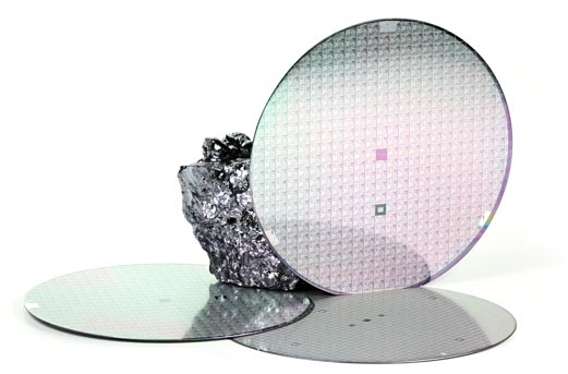
The process begins with a refined silicon wafer sliced from silicon ingot with a purity of 99.9999%. The thin slice goes through a silicon wafer polishing process, where the surface is smoothened and prepared for fabrication.
Photolithography
The thin wafer is then covered with a photoresist mask and exposed to a high-intensity beam of UV light. A circuit map or outline of the microprocessor is formed on the exposed section of the wafer, and the photoresist is washed off using a solvent.
Doping
After photolithography, the wafer is bombarded with trivalent and pentavalent ions to change the semi-conductive properties of the silicon along the circuit map through a process called doping. Boron, germanium, and gallium are some of the most popular elements used in doping.
Etching
Etching is the process of forming physical ridges and troughs in the silicon wafer to create and separate the actual transistors and gates. There are generally two types of etching; one is wet etching that uses chemical solutions to corrode specific sections of the surface, and dry etching where the etching material is dissolved in the silicon using vapor or reactive ions.
Electroplating and Layering
The wafer is placed in an electroplating bath, where copper is deposited onto specific contact points. The copper forms interconnect joints and bridges, joining all the various transistors and diodes. The various components are then layered depending on the build architecture of the microprocessor. At this stage, the entire microprocessor architecture has taken shape and can even function.
The final stage is packaging and finally testing. The packaging largely depends on the application of the microchip. It dictates the connectivity interface, system requirements, compatibility, and other useful features such as mounting and cooling.


Leave a Reply